Core interest
The primary object of interest in our group is the electron. The photon follows closely. We make them play in nanostructures, study their behaviour, and try to devise and develop applications based on what we learn.
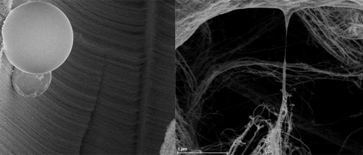
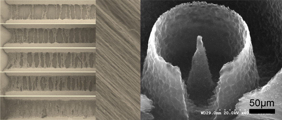
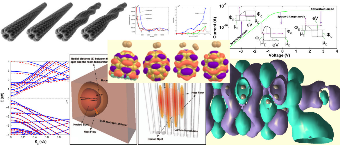
The reduced dimensionality of nanostructures and the strong manifestation of quantum effects in them lead to interesting phenomena and a plethora of possibilities for studying fundamental physics and applying the knowledge gained in order to create new devices and enable new technologies. At its core, our group’s research involves fabricating and exploring nanostructures, with emphasis on the interaction of electrons and photons with and in them. Of course, often phonons may also be involved, or possibly other quasiparticles or collective excitations. More specifically, we investigate the movement of electrons over and through energy barriers, both within solids and into a vacuum, using excitation by heat, light, field, or other electrons. We thus study both solid-state and vacuum devices, as well as the interface between the solid and vacuum, where many interesting things happen. Our primary nanomaterial of interest is the carbon nanotube, although we also work with nanostructures of other materials as needed. To gain a better feel for our works, click here and here for brief videos of our lab, and here and here for two research talks by Alireza Nojeh.
Application areas
* Energy exchange and conversion: This area is concerned with the investigation of energy exchange mechanisms at the mesoscale and nanoscale and the creation of devices for the efficient conversion of heat-to-electricity and light-to-heat-to-electricity. For example, based on an unusual light-induced heating mechanism in arrays of carbon nanotubes (the “Heat Trap” effect) discovered by our group, we demonstrated a compact thermionic solar cell – something that had not been possible in the past using bulk materials. Our work in this area includes both experiment and theory.
* Nanoelectronics and free-electron devices: This area involves solid-state and vacuum nanoelectronics, with emphasis on electron emission and transport as the foundational blocks of vacuum electronics. For example, this includes creating novel electron sources that could be applied in electron microscopy, electron-beam lithography, free-electron lasers, terahertz sources, or machining technologies. Another aspect of this work includes the study of the imaging mechanisms of nanostructures in electron microscopy. Our work in this area includes both experiment and theory.
* Nanostructure modelling: This area focuses on using computational methods and tools, both quantum and classical, to study a variety of applications. For example, this can include new nanostructure properties, thermal transport, energy storage, electronics, or sensing.
Daily activities
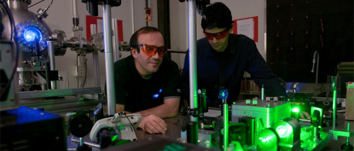
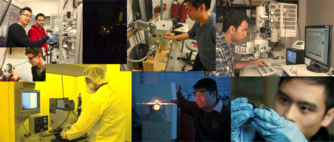
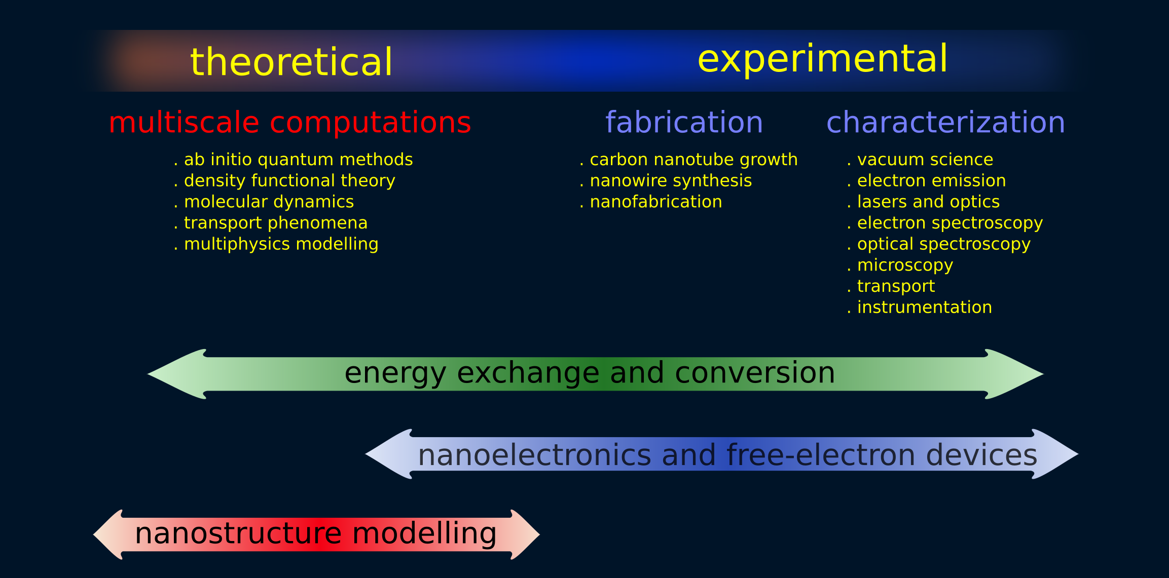
The everyday work in our group is diverse and can involve device design, micro/nanofabrication in the cleanroom, nanostructure growth and deposition, electron and scanning-probe microscopy, building experimental apparatus such as high- or ultra-high-vacuum systems, electronic characterization and sensitive instrumentation, and working with lasers and optics. We complement our experimental efforts with modelling and simulation using methods ranging from continuum modelling (such as finite-element analysis) to classical molecular dynamics to first-principles, quantum-mechanical techniques like the Hartree-Fock theory, configuration-interaction, perturbation theory, and the density-functional theory.
The diagram below summarizes our research areas and the activities involved in them.
Associations
Our research group is part of UBC‘s Department of Electrical and Computer Engineering, Stewart Blusson Quantum Matter Institute, Advanced Materials and Process Engineering Laboratory, and Microsystems and Nanotechnology Group; we are also associated with the Institute for Computing, Information and Cognitive Systems.